Suntan hot offer Trimming Potentiometer-3323
 Comments(0)
 Suntan offer full kinds of Trimming Potentiometer as below. Please check http: / / http://www.suntan.com.hk/Trimming-Potentiometers/ for data sheet freely.
TSR-3006 - Rectangular 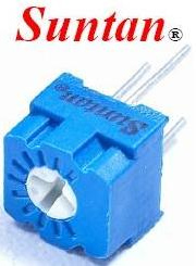 Trimming Potentiometer
TSR-3323 - 4 Terminal Square Trimming Potentiometer
TSR-3296 - 5 Terminal Square Trimming Potentiometer
TSR-3362 - 7 Terminal Square Trimming Potentiometer
TSR-3386 - 8 Terminal Square Trimming Potentiometer
TSR-3329 - Circularity Trimming Potentiometer
TSR-3266 - 5 Terminal Square Trimming Potentiometer
TSR-3318 - 6mm Phenolic Round Trimming Potentiometer
TSR-3306 - 6mm Cermet Round Trimming Potentiometer
TSR-3309 - 9mm Round Trimming Potentiometer
TSR-065 - Phenolic Trimming Potentiometer
TSR-3590 - Precision Multiturn Wirewound Potentiometer
TSR-105H - 6 Terminal Trimming Potentiometer
Delivery: 2 weeks
Packing information: 50pcs/ tube
MOQ: 500 pcs